ADC Peripheral
Analog-to-Digital Converters (ADCs) translate analog signals (e.g., from sensors or microphones) into digital form, readable by CPU.
The STM32H747 features three 16-bit ADCs with up to 20 multiplexed channels each.
Errors
The main ADC error code prefix is 0x20xx. Find the way to display errors in your Arduino sketch here.
An overview of possible errors for ADC:
0x2000: No Errors0x2001: ADC was initialized before initialization0x2002: Passed ADC instance is not eitherADC1,ADC2norADC30x2003: ADC failed to disable0x2004: ADC failed to power up0x2005: Selected pin for ADC is not reachable. Refer to the table to find proper pins for each ADC instance0x2006: Unexpected pin number during initialization. Must be at least 10x2007: Unexpected address or memory size for DMA0x2008: Unexpected sampling frequency. Must be at least 1kHz0x2009: Software polling inSENSEDU_ADC_MODE_ONE_SHOTis currently broken. UseSENSEDU_ADC_MODE_CONTorSENSEDU_ADC_MODE_CONT_TIM_TRIGGERED. If you want to look into this and have a try fixing it, refer to this issue
An overview of critical errors. They shouldn’t happen in normal user case and indicate some problems in library code:
0x20A0: PLL configuration failed0x20A1: Internal logic for channel selection failed0x20A1: Internal logic for setting sample time failed0x20A2: Operation mode selection accepted unexpected value. Should never happen, since all possible values of typeSENSEDU_ADC_CONVMODEmust be handled internally0x20A3: Data management mode selection accepted unexpected value. Should never happen, since all possible values of typeSENSEDU_ADC_DMAmust be handled internally
Structs
SensEdu_ADC_Settings
ADC configuration structure.
typedef struct {
    ADC_TypeDef* adc;
    uint8_t* pins;
    uint8_t pin_num;

    SENSEDU_ADC_CONVMODE conv_mode;
    uint32_t sampling_freq;

    SENSEDU_ADC_DMA dma_mode;
    uint16_t* mem_address;
    uint16_t mem_size;
} SensEdu_ADC_Settings;
Fields
adc: Selects the ADC peripheral (ADC1,ADC2orADC3)pins: Array of Arduino-labeled analog pins (e.g., {A0,A3,A7}). The ADC will sequentially sample these pinspin_num:pinsarray lengthconv_mode:SENSEDU_ADC_MODE_ONE_SHOT: Single conversion on demandSENSEDU_ADC_MODE_CONT: Continuous conversionsSENSEDU_ADC_MODE_CONT_TIM_TRIGGERED: Timer-driven continuous conversions, which enables stable sampling frequency
sampling_freq: Specified sampling frequency forSENSEDU_ADC_MODE_CONT_TIM_TRIGGEREDmode. Up to 1MS/secdma_mode: Specifies if ADC values are manually polled with CPU or automatically transferred into memory with DMA:SENSEDU_ADC_DMA_CONNECT: Attach DMASENSEDU_ADC_DMA_DISCONNECT: CPU polling
mem_address: DMA buffer address in memory (first element of the array)mem_size: DMA buffer size
Notes
Be aware of which pins you can use with selected ADC. Table below shows ADC connections. For example, you can’t access ADC3 with pin A7, cause it is only connected to ADC1.
ADCx_INPy:x: Connected ADCs (e.g.,ADC12_INP4-ADC1andADC2)y: Channel index
| Arduino Pin | STM32 GPIO | Available ADCs |
|---|---|---|
| A0 | PC4 | ADC12_INP4 |
| A1 | PC5 | ADC12_INP8 |
| A2 | PB0 | ADC12_INP9 |
| A3 | PB1 | ADC12_INP5 |
| A4 | PC3 | ADC12_INP13 |
| A5 | PC2 | ADC123_INP12 |
| A6 | PC0 | ADC123_INP10 |
| A7 | PA0 | ADC1_INP16 |
| A8 | PC2_C | ADC3_INP0 |
| A9 | PC3_C | ADC3_INP1 |
| A10 | PA1_C | ADC12_INP1 |
| A11 | PA0_C | ADC12_INP0 |
Functions
SensEdu_ADC_Init
Configures ADC clock and initializes peripheral with specified settings (channels, sampling frequency, etc.).
void SensEdu_ADC_Init(SensEdu_ADC_Settings* adc_settings);
Parameters
adc_settings: ADC configuration structure
Notes
- Initializes associated DMA and timer in
SENSEDU_ADC_DMA_CONNECTandSENSEDU_ADC_MODE_CONT_TIM_TRIGGEREDmodes respectively.
Be careful to initialize each required ADC before enabling. Certain configuration is shared between multiple ADCs, which could be edited only if related ADCs are disabled.
// ERROR
SensEdu_ADC_Init(ADC1_Settings);
SensEdu_ADC_Enable(ADC1);
SensEdu_ADC_Init(ADC2_Settings);
SensEdu_ADC_Enable(ADC2);

// CORRECT
SensEdu_ADC_Init(ADC1_Settings);
SensEdu_ADC_Init(ADC2_Settings);
SensEdu_ADC_Enable(ADC1);
SensEdu_ADC_Enable(ADC2);
SensEdu_ADC_Enable
Powers on the ADC.
void SensEdu_ADC_Enable(ADC_TypeDef* ADC);
Parameters
ADC: ADC Instance (ADC1,ADC2orADC3)
Notes
- Enables sampling frequency timer in
SENSEDU_ADC_MODE_CONT_TIM_TRIGGEREDmode. - Don’t confuse with
SensEdu_ADC_Start.Enableturns ADC on, butStartis used to trigger conversions.
SensEdu_ADC_Disable
Deactivates the ADC.
void SensEdu_ADC_Disable(ADC_TypeDef* ADC);
Parameters
ADC: ADC Instance (ADC1,ADC2orADC3)
Notes
- Disables associated DMA in
SENSEDU_ADC_DMA_CONNECTmode.
SensEdu_ADC_Start
Triggers ADC conversions.
void SensEdu_ADC_Start(ADC_TypeDef* ADC);
Parameters
ADC: ADC Instance (ADC1,ADC2orADC3)
Notes
- Enables associated DMA in
SENSEDU_ADC_DMA_CONNECTmode.
SensEdu_ADC_GetTransferStatus
Returns current DMA transfer status (dma_complete flag)
uint8_t SensEdu_ADC_GetTransferStatus(ADC_TypeDef* adc);
Parameters
ADC: ADC Instance (ADC1,ADC2orADC3)
Returns
dma_completeflag:HIGHindicated that DMA controller finished memory transfer
Notes
dma_completeflag is automatically cleared by callingSensEdu_ADC_Start()
Avoid performing any actions without acknowledging this flag. It ensures that the data was completely transferred.
SensEdu_ADC_ReadConversion
Manually read a single ADC conversion (alternative to DMA).
uint16_t SensEdu_ADC_ReadConversion(ADC_TypeDef* ADC)
Parameters
ADC: ADC Instance (ADC1,ADC2orADC3)
Returns
- 16-bit value from selected channel
Notes
- Used for readings using single channel. For multi-channel readings, use
SensEdu_ADC_ReadSequence. - Consumes CPU cycles. Prefer DMA to free CPU for other tasks. For example, you can perform complex calculations on ADC values, while requesting the new set of data with DMA.
- Refer to non-DMA examples like
Read_ADC_1CH.
SensEdu_ADC_ReadSequence
Manually read a sequence of ADC conversions (alternative to DMA).
uint16_t SensEdu_ADC_ReadSequence(ADC_TypeDef* ADC)
Parameters
ADC: ADC Instance (ADC1,ADC2orADC3)
Returns
- A pointer to an array of ADC conversion results. Index the array to access values:
[0],[1],[2], etc., corresponding to the amount of selected channels (pinsarray inSensEdu_ADC_Settings)
Notes
- Used for readings using multiple channels. For single-channel readings, use
SensEdu_ADC_ReadConversion. - Consumes CPU cycles. Prefer DMA to free CPU for other tasks. For example, you can perform complex calculations on ADC values, while requesting the new set of data with DMA.
- Refer to non-DMA examples like
Read_ADC_3CH.
Multi-channel CPU polling currently doesn’t work in SENSEDU_ADC_MODE_ONE_SHOT. Use SENSEDU_ADC_MODE_CONT or SENSEDU_ADC_MODE_CONT_TIM_TRIGGERED. If you want to look into this and have a try fixing it, refer to this issue.
SensEdu_ADC_ShortA4toA9
Shorts pin A4 to A9 on Arduino.
void SensEdu_ADC_ShortA4toA9(void);
Notes
- In older board revisions, microphone #2 is wired to pin
A9(PC3_C), which is routed only toADC3. This conflicts with project requiring x4 microphones, usingADC1andADC2with x2 channels per ADC. To solve this problem,_Cpins could be shorted to theirnon_Ccounterparts. This way pinA4(PC3) is bridged toA9(PC3_C), allowing microphone #2 to be accessed via any ADC, sincePC3is shared betweenADC1andADC2. Refer to the table at settings section for better understanding.
Examples
Examples are organized incrementally. Each builds on the previous one by introducing only new features or modifications. Refer to earlier examples for core functionality details.
If you want to see complete examples, visit \examples\ directory or open them via Arduino IDE by navigating to File → Examples → SensEdu.
Read_ADC_1CH
Continuously reads ADC conversions directly via CPU for one selected analog pin.
- Include SensEdu library
- Declare ADC instance, pin array and array size corresponding to your channel count for selected ADC
- Configure ADC Parameters by declaring
SensEdu_ADC_Settingsstruct - Initialize
SensEdu_ADC_Init()and power up ADCSensEdu_ADC_Enable() - Start ADC once with
SensEdu_ADC_Start()(once applies only for continuous modeSENSEDU_ADC_MODE_CONT) - In a loop, manually read data from a single channel using
SensEdu_ADC_ReadConversion(). Print results withSerial - Open Serial Monitor to see results. Try to connect selected pin to GND or 3.3V. The values should vary in a range from 0 to 65535
#include "SensEdu.h"

ADC_TypeDef* adc = ADC1;
const uint8_t adc_pin_num = 1;
uint8_t adc_pins[adc_pin_num] = {A0};
SensEdu_ADC_Settings adc_settings = {
    .adc = adc,
    .pins = adc_pins,
    .pin_num = adc_pin_num,

    .conv_mode = SENSEDU_ADC_MODE_CONT,
    .sampling_freq = 0,

    .dma_mode = SENSEDU_ADC_DMA_DISCONNECT,
    .mem_address = 0x0000,
    .mem_size = 0
};

void setup() {
    Serial.begin(115200);

    SensEdu_ADC_Init(&adc_settings);
    SensEdu_ADC_Enable(adc);
    SensEdu_ADC_Start(adc);
}

void loop() {
    uint16_t data = SensEdu_ADC_ReadConversion(adc);
    Serial.println(data);
}
Notes
- For the most simple CPU polling configuration there are unused parameters like
.sampling_rateor.mem_address. Such parameters could be set to any value, they are completely ignored. - ADC values are 16-bit, vary from 0 (0V) to 65535 (3.3V).
Read_ADC_3CH
Continuously reads sequences of ADC conversions directly via CPU for multiple selected analog pins.
- Follow base configuration from the
Read_ADC_1CHexample - Expand pin array to include all desired channels. Update array size to match channel count
- Use
SensEdu_ADC_ReadSequence()to retrieve a channel sequence array
...
const uint8_t adc_pin_num = 3;
uint8_t adc_pins[adc_pin_num] = {A0, A1, A2};
...
void loop() {
    uint16_t* data = SensEdu_ADC_ReadSequence(adc);
    Serial.println("-------");
    for (uint8_t i = 0; i < adc_pin_num; i++) {
        Serial.print("Value CH");
        Serial.print(i);
        Serial.print(": ");
        Serial.println(data[i]);
    }
}
Notes
- Compared to single-channel configuration,
SensEdu_ADC_ReadSequence()returns not a value, but a pointer. Using this pointer, you can access all channels in a sequence with index brackets[]. - ADC conversions are organized in a “package” called sequence. They follow exact order defined in
adc_pins(A0 → A1 → A2 in this example).
Read_ADC_1CH_TIM
Continuously reads ADC conversions directly via CPU for one selected analog pin with constant sampling rate using timer trigger.
- Follow base configuration from the
Read_ADC_1CHexample - Update conversion mode
.conv_modeinSensEdu_ADC_SettingstoSENSEDU_ADC_MODE_CONT_TIM_TRIGGERED - Specify sampling frequency in Hz via
.sampling_freq
...
SensEdu_ADC_Settings adc_settings = {
    .adc = adc,
    .pins = adc_pins,
    .pin_num = adc_pin_num,

    .conv_mode = SENSEDU_ADC_MODE_CONT_TIM_TRIGGERED,
    .sampling_freq = 250000,

    .dma_mode = SENSEDU_ADC_DMA_DISCONNECT,
    .mem_address = 0x0000,
    .mem_size = 0
};
...
Notes
- Expect small variations from specified sampling frequency
Read_ADC_3CH_TIM
Continuously reads sequences of ADC conversions directly via CPU for multiple selected analog pins with constant sampling rate using timer trigger.
- Follow base multi-channel configuration from the
Read_ADC_3CHexample - Update conversion mode
.conv_modeinSensEdu_ADC_SettingstoSENSEDU_ADC_MODE_CONT_TIM_TRIGGERED - Specify sampling frequency in Hz via
.sampling_freq
...
SensEdu_ADC_Settings adc_settings = {
    .adc = adc,
    .pins = adc_pins,
    .pin_num = adc_pin_num,

    .conv_mode = SENSEDU_ADC_MODE_CONT_TIM_TRIGGERED,
    .sampling_freq = 250000,

    .dma_mode = SENSEDU_ADC_DMA_DISCONNECT,
    .mem_address = 0x0000,
    .mem_size = 0
};
...
Notes
- Expect small variations from specified sampling frequency
Read_ADC_1CH_DMA
Continuously reads ADC conversions using DMA for a single analog pin, allowing efficient data transfer without CPU intervention.
- Follow the base configuration from the
Read_ADC_1CHexample - Declare ADC Buffer with a macro
SENSEDU_ADC_BUFFERto store the data. It takes two parameters: the user-defined name to be used in the code and the buffer size (number of elements) - In
SensEdu_ADC_Settings, set.dma_modetoSENSEDU_ADC_DMA_CONNECT - Assign
.mem_addressto the buffer’s first element address and.mem_sizeto its length - After calling
SensEdu_ADC_Start(), the ADC fills the buffer with conversions and automatically stops, setting thedma_completeflag - Check
dma_completeusingSensEdu_ADC_GetTransferStatus(). Whentrue, read the buffer and perform operations (e.g., print values, compute something) - Call
SensEdu_ADC_Start()again to trigger the next ADC-DMA sequence
#include "SensEdu.h"

const uint16_t memory4adc_size = 128;
SENSEDU_ADC_BUFFER(memory4adc, memory4adc_size);

ADC_TypeDef* adc = ADC1;
const uint8_t adc_pin_num = 1;
uint8_t adc_pins[adc_pin_num] = {A0};
SensEdu_ADC_Settings adc_settings = {
    .adc = adc,
    .pins = adc_pins,
    .pin_num = adc_pin_num,

    .conv_mode = SENSEDU_ADC_MODE_CONT,
    .sampling_freq = 0,

    .dma_mode = SENSEDU_ADC_DMA_CONNECT,
    .mem_address = (uint16_t*)memory4adc,
    .mem_size = memory4adc_size
};

void setup() {
    Serial.begin(115200);

    SensEdu_ADC_Init(&adc_settings);
    SensEdu_ADC_Enable(adc);
    SensEdu_ADC_Start(adc);
}

void loop() {
    // do something else when transfer is not yet completed
    if (SensEdu_ADC_GetTransferStatus(adc)) {
        Serial.println("------");
        for (int i = 0; i < memory4adc_size; i++) {
            Serial.print("ADC value ");
            Serial.print(i);
            Serial.print(": ");
            Serial.println(memory4adc[i]);
        };

        SensEdu_ADC_Start(adc);
    }
}
Notes
SensEdu_ADC_Start()resets thedma_completeflag automatically.- Optimize your code to use DMA capability to perform memory transfers in the background. For example, start a new measurement in the middle of calculations, when the whole old dataset is not needed anymore.
Always use SENSEDU_ADC_BUFFER macro to define arrays for ADC in DMA mode. This macro automatically handles all buffer requirements for cache coherence, regardless of the selected size. For details, visit the Cache Coherence section.
Read_ADC_3CH_DMA
Continuously reads ADC conversions using DMA multiple selected analog pins, allowing efficient data transfer without CPU intervention.
- Follow the DMA configuration from the
Read_ADC_1CH_DMAexample - Expand pin array to include all desired channels. Update array size to match channel count
- Expand the ADC DMA buffer accordingly to include data for all channels
- Data is organized in a sequence, following the order defined in pin array (e.g., A0 → A1 → A2 → A0 → A1 → …)
...
const uint8_t adc_pin_num = 3;
uint8_t adc_pins[adc_pin_num] = {A0, A1, A2};

const uint16_t memory4adc_size = 64 * adc_pin_num;
SENSEDU_ADC_BUFFER(memory4adc, memory4adc_size);
...
void loop() {
    // do something else when transfer is not yet completed
    if (SensEdu_ADC_GetTransferStatus(adc)) {
        Serial.println("------");
        for (int i = 0; i < memory4adc_size; i+=3) {
            Serial.print("ADC value ");
            Serial.print(i/3);
            Serial.print("CH1: ");
            Serial.println(memory4adc[i]);

            Serial.print("ADC value ");
            Serial.print(i/3);
            Serial.print("CH2: ");
            Serial.println(memory4adc[i+1]);

            Serial.print("ADC value ");
            Serial.print(i/3);
            Serial.print("CH3: ");
            Serial.println(memory4adc[i+2]);
        }

        SensEdu_ADC_Start(adc);
    };
}
Read_2ADC_3CH_DMA
This example demonstrates the usage of multiple ADCs in DMA mode. Essentially, you follow the same steps as in the Read_ADC_3CH_DMA example, but use separate buffers, configuration structures, and function calls for each ADC.
For example:
SensEdu_ADC_Init(&adc1_settings);
SensEdu_ADC_Enable(ADC1);
SensEdu_ADC_Start(ADC1);

SensEdu_ADC_Init(&adc2_settings);
SensEdu_ADC_Enable(ADC2);
SensEdu_ADC_Start(ADC2);
Notes
- Ensure there is no pin overlap between different ADCs (e.g., do not include pin A0 in the arrays for both ADC1 and ADC2).
Developer Notes
DMA Streams
Each ADC occupies one DMA stream:
- ADC1: DMA1_Stream6
- ADC2: DMA1_Stream5
- ADC3: DMA1_Stream7
Avoid reusing occupied DMA streams. Refer to STM32H747 Reference Manual to find free available streams.
Reading ADC Data
The STM32H7 microcontroller is equipped with three ADC modules, each capable of accessing multiple channels (refer to the ADC mapping table above). Reading the ADC values from a single channel is straightforward, as the data is stored consecutively in an array.
However, when reading data from multiple channels within a single ADC module, users must use different approach. The data for each channel is interleaved in the array, meaning that the data for each channel is stored one after the other, rather than all data from first channel followed by all data from second channel, and so forth. This structure is illustrated clearly in the following figure giving an example of using two channels with one ADC module.

Conversion Time
You can calculate the needed time for each conversion \((T_{CONV})\) with this formula:
\[T_{CONV} = T_{SMPL} + T_{SAR}\]- \(T_{SMPL}\): Configured sampling time
- \(T_{SAR}\): Successive approximation time depending on data resolution
In SensEdu, \(T_{SMPL}\) is configured to \(2.5\) ADC clock cycles, which correpsonds to bits SMP[2:0] = 0b001 in the ADC_SMPR1 and ADC_SMPR2 registers.
ADC conversions are fixed to 16-bit resolution, so \(T_{SAR}\) is constant and equals to \(8.5\) ADC clock cycles.
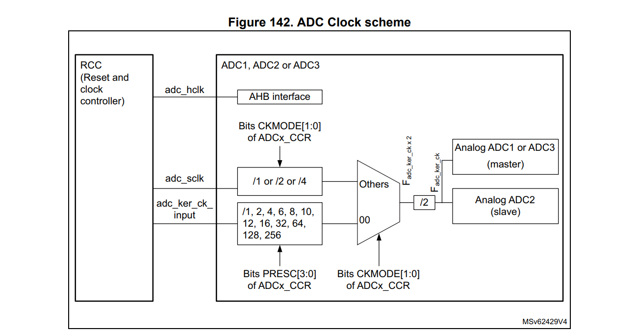
The ADC clock is routed from the PLL2 clock and set to \(25\text{MHz}\) for each individual ADC, which gives us:
\[T_{CONV} = (2.5 \text{ cycles} + 8.5 \text{ cycles}) * \frac{1}{f_{\text{adc_ker_ck}}} = 11 \text{ cycles} * \frac{1}{25\text{MHz}} = 440\text{ns}\]SensEdu is configured to x2 oversampling (basically, averaging), so we require around \(880\text{ns}\) per one ADC conversion, which theoretically gives us a maximum \(1136\text{kS/sec}\) sampling rate. Based on the practical tests of the ADC sampling rate, the theoretical maximum of the sampling rate can be achieved with a negligible error that is the result of various additional delays. Therefore, the practical limit of the ADC sampling rate is set to \(1000\text{kS/sec}\) which corresponds to a sampling frequency of \(1\text{MHz}\). Any attempt to increase this rate further results in a decrease in the actual sampling rate of the module.
Initialization
General ADC configuration:
| Register name | Register Field | Value | Manual Page | Function |
|---|---|---|---|---|
| CR | BOOST | 0b10 | 26.4.3 Page: 958 | ADC clock range \(12.5\text{MHz}:25\text{MHz}\) |
| CFGR | RES | 0b000 | 26.6.4 Page: 1047 | 16-bit Resolution |
| CFGR | OVRMOD | 0b1 | 26.4.27 Page: 998 | Overrun mode (overwrite data) |
| SMPRx | SMPy | 0b001 | 26.4.13 Page: 972 | Sample Time of 2.5 ADC clock cycles |
| CFGR2 | OVSR | 2U - 1U | 26.4.31 Page: 1009 | x2 Oversampling |
| CFGR2 | ROVSE | 0b1 | 26.4.31 Page: 1009 | Enable Oversampling |
| CFGR2 | OVSS | 0b0001 | 26.4.31 Page: 1009 | 1-bit right shift to account for x2 oversampling (averaging) |
DMA vs CPU polling specific:
| CFGR | DMNGT | 0b01 | 26.4.27 Page: 1000 | DMA is enabled in circular mode |
| CFGR | DMNGT | 0b00 | 26.4.27 Page: 1000 | Data is stored only in Data Register (DR) |
Timer triggered mode (sampling rate generation) specific:
| CFGR | EXTEN | 0b01 | 26.4.19 Page: 977 | Enable trigger on rising edge |
| CFGR | EXTSEL | depends on TIMx | 26.4.19 Page: 977 | Code for selected timer that triggers ADC conversions |
Continuous mode specific:
| CFGR | CONT | 0b0 | 26.4.14 Page: 973 | Single conversion mode (SENSEDU_ADC_MODE_ONE_SHOT)
|
| CFGR | CONT | 0b1 | 26.4.15 Page: 973 | Continuous conversion mode (SENSEDU_ADC_MODE_CONT)
|
Clock Configuration
To configure the ADC clock, it is first necessary to configure the PLL (Phase-Locked Loop). The PLL contains frequency multipliers and dividers that enable the generation of different frequencies, which are multiples of the input frequency.
The source frequency for the PLL is the HSE (High Speed External Oscillator), which has a frequency of 16MHz.
The clock is first divided by DIVM2, which is set to 4, resulting in a 4MHz PLL2 input frequency (\(\text{ref2_ck}\)). Additionally, the PLL2RGE field in the PLLCFGR register must be configured according to the selected range for \(\text{ref2_ck}\). Since we use 4MHz, it is set to the 4:8MHz range.
The clock is then multiplied by DIVN2, which is set to 75, resulting in a VCO (Voltage-Controlled Oscillator) frequency of 300MHz. The frequency was selected to fit within the chosen VCO range in the PLL2VCOSEL field of the PLLCFGR register, which is set to the narrow range of 150:420MHz.
Finally, the VCO frequency is divided by DIVP2, which is set to 6, resulting in a 50MHz frequency for the shared ADC bus.
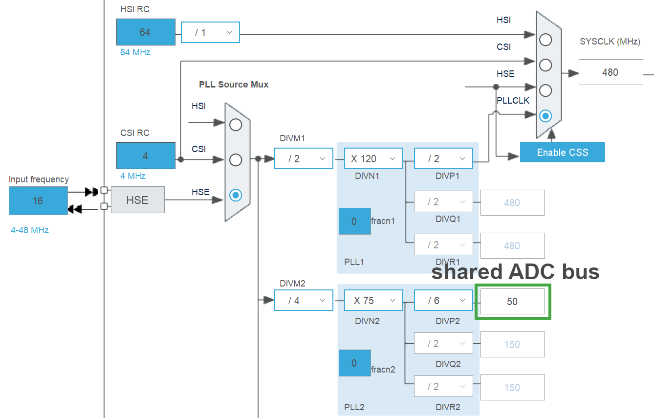
The ADC clock is selected to be independent and asynchronous with the AHB clock, named \(\text{adc_ker_ck_input}\) and derived from PLL2. The clock then passes through a settable prescaler CKMODE in the ADCx_CCR register, which is set to 1 (no clock division). Then, it passes through a fixed /2 prescaler, resulting in a 25MHz frequency (\(F_{\text{adc_ker_ck}}\)) for each individual ADC. This frequency must comply with the maximum ADC clock frequency specified in Table 99 of the STM32H747 Datasheet.
Cache Coherence
When using the ADC with DMA, you must account for data cache (D‑Cache) coherence. The DMA controller writes samples directly to memory, bypassing the CPU and therefore not updating the cache. If CPU then reads the buffer from cache, it may read outdated samples stored in cache instead of the actual data in memory, as it is not aware of DMA transfers.
To ensure the CPU reads fresh data, invalidate the D-Cache lines that cover the DMA destination buffer. Use the CMSIS function SCB_InvalidateDCache_by_Addr(mem_addr, mem_size), where:
mem_addr: the start address of the ADC buffer (aligned to a cache-line boundary)mem_size: the length in bytes
Invalidation operates on whole cache lines. If the buffer is not aligned or its size is not a multiple of the cache-line size, invalidation may affect cache lines that also contain unrelated variables, which can degrade performance.
To avoid that, align the ADC buffer to the cache-line size and choose a buffer length that is a cache-line multiple. On STM32H747, the D-Cache line size is 32 bytes and is available as the macro __SCB_DCACHE_LINE_SIZE. For a uint16_t buffer, the element count should be a multiple of 16. A properly aligned manual declaration looks like this:
const uint16_t memory4adc_size = 128; // multiple of __SCB_DCACHE_LINE_SIZE/sizeof(uint16_t)
__attribute__((aligned(__SCB_DCACHE_LINE_SIZE))) uint16_t memory4adc[memory4adc_size];
The SensEdu library automates both proper buffer declaration and cache invalidation. Use the following procedure:
- Declare the buffer with
SENSEDU_ADC_BUFFER(name, user_size)where:name: the variable name to access the buffer later in codeuser_size: the number of requireduint16_telements
- Start the ADC with
SensEdu_ADC_Start(ADC_TypeDef* ADC)after initialization
The library:
- Ensures the buffer is aligned to
__SCB_DCACHE_LINE_SIZE - Rounds the actual allocation as needed to satisfy cache-line requirements
- Performs the required cache invalidation automatically inside
SensEdu_ADC_Start(ADC_TypeDef* ADC)before starting DMA transfers
const uint16_t buf_size = 50;
uint8_t pins[1] = {A0};
SENSEDU_ADC_BUFFER(buf, buf_size);
SensEdu_ADC_Settings adc_settings = {
    .adc = ADC1,
    .pins = pins,
    .pin_num = 1,
    .conv_mode = SENSEDU_ADC_MODE_CONT,
    .sampling_freq = 0,
    .dma_mode = SENSEDU_ADC_DMA_CONNECT,
    .mem_address = (uint16_t*)buf,
    .mem_size = buf_size
};

void setup() {
    SensEdu_ADC_Init(&adc_settings);
    SensEdu_ADC_Enable(ADC1);
    SensEdu_ADC_Start(ADC1);
}

void loop() {
    if (SensEdu_ADC_GetTransferStatus(ADC1)) {
        Serial.println("------");
        for (uint16_t i = 0; i < buf_size; i++) {
            Serial.println(buf[i]);
        }
        SensEdu_ADC_ClearTransferStatus(ADC1);
        SensEdu_ADC_Start(ADC1);
    }
}
The SENSEDU_ADC_BUFFER macro accepts any user-defined size in uint16_t elements. The library allocates a slightly larger buffer internally to meet cache‑line requirements. Continue to use the requested element count (user_size) ignoring the internally padded capacity.
Some legacy projects manually declare DMA buffers using the __attribute__((aligned(...))). While this can work, it is easy to get alignment or sizing wrong, which can lead to unnecessary cache invalidation or other unexpected behavior. Whenever you use the ADC in DMA mode, prefer SENSEDU_ADC_BUFFER.